PHYSICAL VLSI DESIGN

PHYSICAL VLSI DESIGN

Wishlist Share
Share Course
Page Link
Share On Social Media

About Course

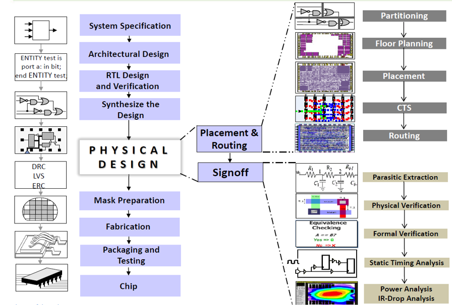
  • Get complete knowledge regarding backend design and physical design flow.
  • Analyze the different steps, such as floorplan, placement, cts, and routing, in the physical design flow.
  • Analysis of timing analysis, congestion, and utilization in each step.
  • Study of physical verification, including design rule check and layout vs schematic.

What Will You Learn?

  • • Learn the basic design flow in VLSI physical design automation.
  • • Analysis of static timing analysis and timing closure.
  • • Analysis of design and characterization technique.
  • • Analysis of different concepts and techniques for optimization.
  • • Identification of issues in physical design.

Course Content

Introduction to ASIC & Physical Design Flow
Inputs of Physical Design, PnR Flow

Floorplan
Sanity Checks, Types, Port and Macro Placement, Macro Guidelines, Utilization Factor, and Aspect Ratio

Power planning
Rings, Straps, Rails, UPF, Scan Chain Re-ordering

Placement
Standard Cells, Optimization, Congestion, Cell Padding, Keepout Margins, DRV’s, Fixes

Clock Tree Synthesis (CTS) & Signal Integrity
High Fanout Net Synthesis, Types of Clock Tree, Insertion Delay, Skew, Latency, Timing Fixes (Setup and Hold)

Routing
Global & Detailed Routing, Physical DRCs

Signoff Stages: Physical Verification
Design Rule Check (DRC), Layout versus Schematic (LVS), RC Extraction

Static Time Analysis (STA) and Timing Closure
Difference Between DTA & STA, Setup & Hold Timing Analysis and Introduction to Flip-Flop Setup Time, Introduction To Clock Jitter and Uncertainty, Fixing Setup & Hold, Clock Domain Crossing, Multi-VT Cells, Power and IR Analysis

Issues In PD
Electromigration, Latch Up, Antenna Effect, Crosstalk

Engineering Change Order (ECO)
Post Route ECO, Post Silicon ECO, Tape Out

Student Ratings & Reviews

No Review Yet
No Review Yet